Toggle light / dark theme

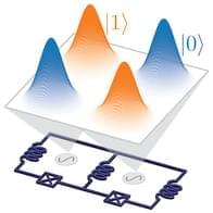
Here we propose a novel protected erasure qubit, the Floquet fluxonium molecule (FFM). The FFM qubit exhibits (i) extremely long predicted logical coherence times and relatively long erasure lifetimes, (ii) a simple superconducting circuit structure, and (iii) high-fidelity single-qubit gates, which are much faster than the coherence timescale. Based on a Floquet-driven pair of inductively coupled fluxonium circuits [13–15], the FFM is a multi-DOF superconducting circuit with engineered, highly coherent quasieigenstates.

Our key technical contribution is a novel form of Floquet protection in a multi-DOF qubit, which strongly suppresses phase-flip errors, removing them at first and second order in the flux noise. The combination of drive and multi-DOF allows the low-lying eigenstates to be disjoint and delocalized with a nonvanishing energy gap. The second-order sweet spot has no analogue in the single-DOF circuits that have been studied thus far [16–18]; in fact, in single-DOF circuits there is a generic trade-off between bit-and phase-flip errors arising from the inability to keep two eigenstates simultaneously disjoint and flux delocalized using accessible circuit QED Hamiltonians [19].

The higher-order phase-flip insensitivity allow the predicted coherence time of the FFM qubit to significantly outperform other multi-DOF circuits. These include the following: the dual-rail erasure transmon, with experimentally achieved logical lifetimes of approximately ms and erasure lifetimes of approximately [12]; the dual-rail cavity, with logical lifetimes predicted [10] (achieved [11]) at approximately ms (3 ms), limited by cavity and ancilla dephasing, and erasure lifetimes of approximately in both cases; and the cold echo qubit, with predicted logical lifetime of ms with erasure rates unreported [8]. Theoretically, we find the FFM exhibits long bit-flip coherence times of approximately 50 ms while suppressing phase flips even further, along with a 500-erasure lifetime.

The AI system is dubbed a “quantum-tunneling deep neural network” and combines neural networks with quantum tunneling. A deep neural network is a collection of machine learning algorithms inspired by the structure and function of the brain — with multiple layers of nodes between the input and output. It can model complex non-linear relationships and, unlike conventional neural networks (which include a single layer between input and output) deep neural networks include many hidden layers.

Quantum tunneling, meanwhile, occurs when a subatomic particle, such as an electron or photon (particle of light), effectively passes through an impenetrable barrier. Because a subatomic particle like light can also behave as a wave — when it is not directly observed it is not in any fixed location — it has a small but finite probability of being on the other side of the barrier. When sufficient subatomic particles are present, some will “tunnel” through the barrier.

After the data representing the optical illusion passes through the quantum tunneling stage, the slightly altered image is processed by a deep neural network.

Not only does God play dice, that great big casino of quantum physics could have far more rooms than we ever imagined. An infinite number more, in fact.

Physicists from the University of California, Davis (UCD), the Los Alamos National Laboratory in the US, and the Swiss Federal Institute of Technology Lausanne have redrawn the map of fundamental reality to demonstrate the way we relate objects in physics could be holding us back from seeing a bigger picture.

For about a century, our understanding of reality has been complicated by the theories and observations that fall under the banner of quantum mechanics. Gone are the days when objects had absolute measures like velocity and position.

PRESS RELEASE — After over a year of evaluation, NIST has selected 14 candidates for the second round of the Additional Digital Signatures for the NIST PQC Standardization Process. The advancing digital signature algorithms are:

NIST Internal Report (IR) 8528 describes the evaluation criteria and selection process. Questions may be directed to [email protected]. NIST thanks all of the candidate submission teams for their efforts in this standardization process as well as the cryptographic community at large, which helped analyze the signature schemes.

Moving forward, the second-round candidates have the option of submitting updated specifications and implementations (i.e., “tweaks”). NIST will provide more details to the submission teams in a separate message. This second phase of evaluation and review is estimated to last 12–18 months.

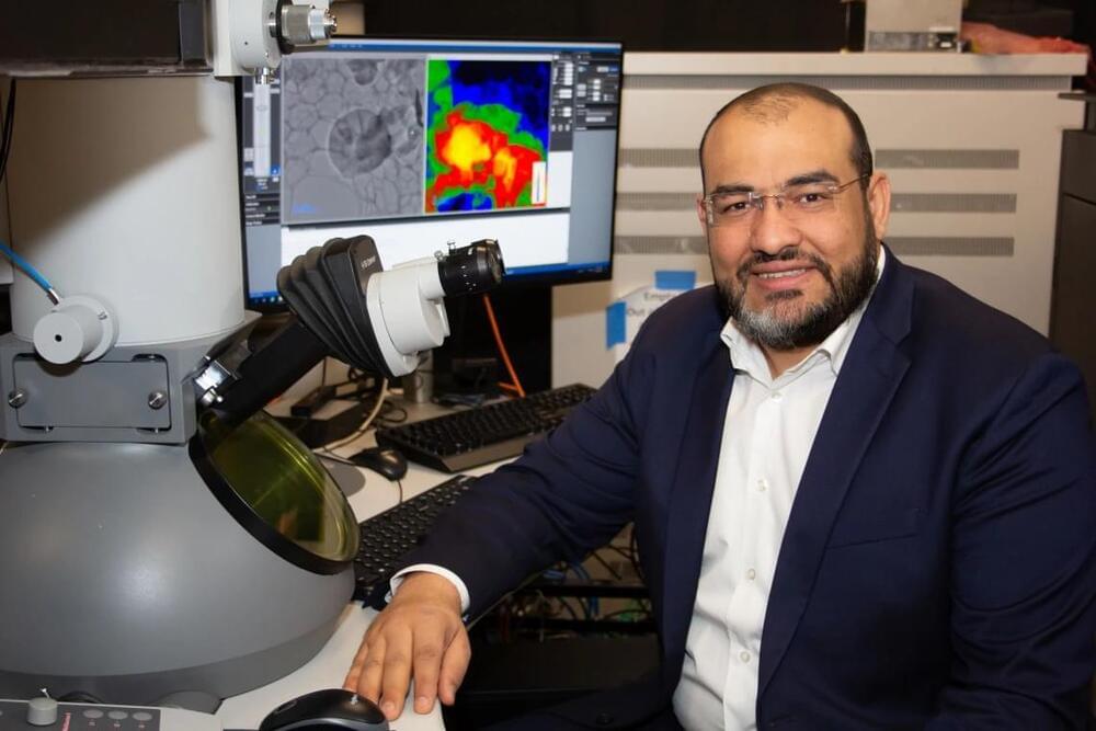
Imagine owning a camera so powerful it can take freeze-frame photographs of a moving electron – an object traveling so fast it could circle the Earth many times in a second. Researchers at the University of Arizona have developed the world’s fastest electron microscope that can do just that.

They believe their work will lead to groundbreaking advancements in physics, chemistry, bioengineering, materials sciences and more.

“When you get the latest version of a smartphone, it comes with a better camera,” said Mohammed Hassan, associate professor of physics and optical sciences. “This transmission electron microscope is like a very powerful camera in the latest version of smartphones; it allows us to take pictures of things we were not able to see before – like electrons. With this microscope, we hope the scientific community can understand the quantum physics behind how an electron behaves and how an electron moves.”