Menu

Blog

Archive for the ‘nanotechnology’ category: Page 50

Feb 9, 2024

A magnetically powered nanomachine with a DNA clutch

Posted by in categories: biotech/medical, nanotechnology

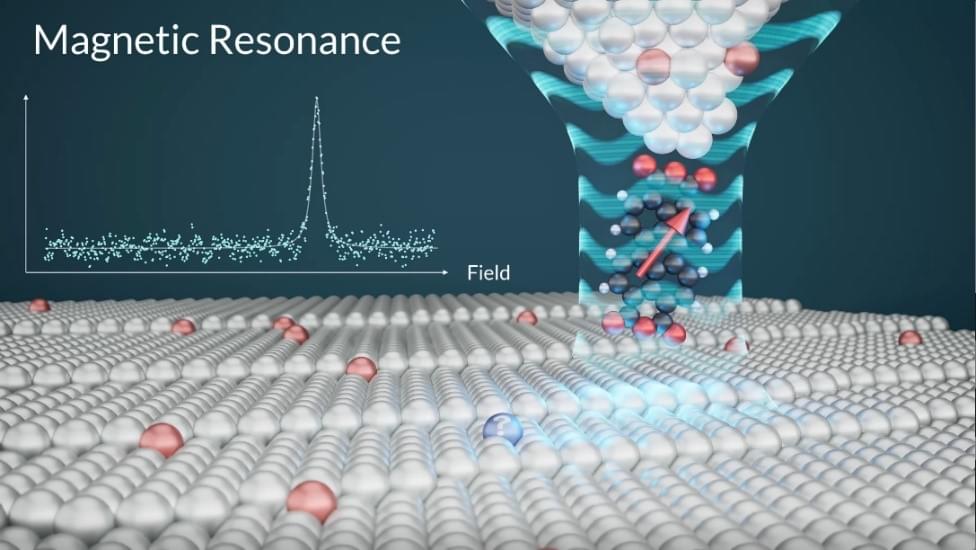
The nanospace confinement of a magnetic nanoparticle within a porous cage, coupled with an encodable DNA clutch interface, enables a remotely powered and controlled rotary nanomotor that is autoresponsive to its microenvironment.

Feb 9, 2024

Beyond cells: Unveiling the potential of genetic circuits on single DNA molecules

Posted by in categories: bioengineering, biotech/medical, genetics, nanotechnology

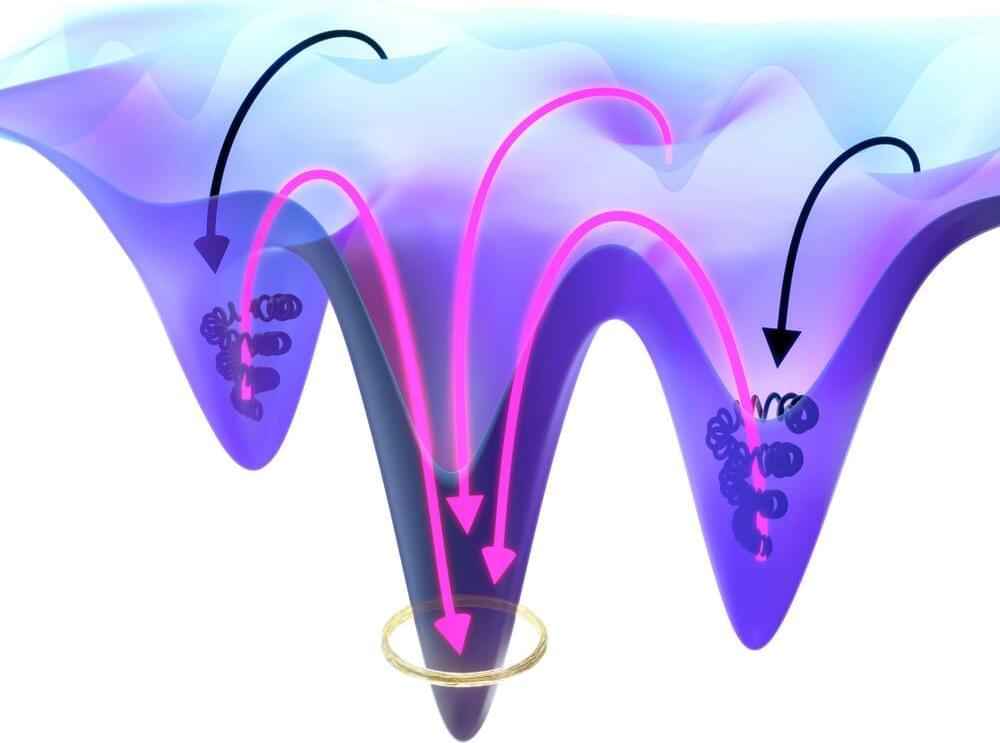
In a new Nature Communications study, researchers have explored the construction of genetic circuits on single DNA molecules, demonstrating localized protein synthesis as a guiding principle for dissipative nanodevices, offering insights into artificial cell design and nanobiotechnology applications.

The term “genetic circuit” is a metaphorical description of the complex network of genetic elements (such as genes, promoters, and ) within a cell that interact to control and cellular functions.

In the realm of artificial cell design, scientists aim to replicate and engineer these genetic circuits to create functional, self-contained units. These circuits act as the molecular machinery responsible for orchestrating cellular processes by precisely regulating the production of proteins and other molecules.

Feb 8, 2024

Revolutionizing Industries With Super-Durable Gold Catalysts

Posted by in categories: materials, nanotechnology

A new protective layer developed by researchers improves gold catalysts’ durability, potentially expanding their industrial applications and efficiency. Credit: SciTechDaily.com.

A protective layer applied to gold nanoparticles can boost its resilience.

For the first time, researchers including those at the University of Tokyo discovered a way to improve the durability of gold catalysts by creating a protective layer of metal oxide clusters. The enhanced gold catalysts can withstand a greater range of physical environments compared to unprotected equivalent materials.

Feb 7, 2024

Building a DNA nanoparticle to be both carrier and medicine

Posted by in categories: bioengineering, biotech/medical, genetics, nanotechnology, robotics/AI

Scientists have been making nanoparticles out of DNA strands for two decades, manipulating the bonds that maintain DNA’s double-helical shape to sculpt self-assembling structures that could someday have jaw-dropping medical applications.

The study of DNA , however, has focused mostly on their architecture, turning the genetic code of life into components for fabricating minuscule robots. A pair of Iowa State University researchers in the genetics, development, and cell biology department—professor Eric Henderson and recent doctoral graduate Chang-Yong Oh—hope to change that by showing nanoscale materials made of DNA can convey their built-in genetic instructions.

“So far, most people have been exploring DNA nanoparticles from an engineering perspective. Little attention has been paid to the information held in those DNA strands,” Oh said.

Feb 6, 2024

Protecting crops through nanotechnology in Southeast Asia

Posted by in categories: biotech/medical, food, nanotechnology

In a recent breakthrough, DNA sequencing technology has uncovered the culprit behind cassava witches’ broom disease: the fungus genus Ceratobasidium. The cutting-edge nanopore technology used for this discovery was first developed to track the COVID-19 virus in Colombia, but is equally suited to identifying and reducing the spread of plant viruses.

The findings, published in Scientific Reports, will help plant pathologists in Laos, Cambodia, Vietnam and Thailand protect farmers’ valued harvest.

“In Southeast Asia, most rely on cassava. Its starch-rich roots form the basis of an industry that supports millions of producers. In the past decade, however, cassava witches’ broom disease has stunted plants, reducing harvests to levels that barely permit affected farmers to make a living,” said Wilmer Cuellar, Senior Scientist at the Alliance of Bioversity and CIAT.

Feb 6, 2024

Anisotropic carrier dynamics and laser-fabricated luminescent patterns on oriented single-crystal perovskite wafers

Posted by in categories: computing, nanotechnology

Based on the differently oriented MAPbBr3 single-crystal wafers, this study presents innovative findings primarily in two aspects. First, utilizing polarization-dependent ultrafast time-resolved spectroscopy, the anisotropic dynamics of photoexcited carriers on the picosecond timescale was first revealed. This discovery provides a deeper understanding of the ultrafast carrier relaxation pathways from the perspective of crystal orientation. It holds significant implications for exploring and expanding the potential of perovskite single crystals in polarization-sensitive and ultrafast optoelectronics applications, such as optical modulators, high-speed light polarization sensors, and ballistic transistors, which require both polarization sensitivity and high-field running capability simultaneously. However, a comprehensive understanding to correlate the observed polarization-dependent dynamics with the crystallographic structures has not been achieved yet due to limitations in current excited-state experimental techniques. Further progress will rely on employing more advanced ultrafast probing techniques, in combination with theoretical simulations, to comprehensively elucidate the observed carrier dynamics behind the underlying excited structure.

Second, by employing femtosecond laser processing, luminescent patterns with a remarkable three-order-of-magnitude PL enhancement on the bulk single crystals were achieved. The observed enhancement can be ultimately attributed to the synergy of three factors: the limited carrier diffusion length, the increase in shallow trap-assisted recombination centers, and the passivation of deep traps within the femtosecond laser-induced tentacle-like microstructures. In addition to offering a convenient top-down strategy for enhancing the photoluminescence intensity of bulk crystals, this study has also provided an in-depth understanding of the luminescence mechanism from multiple spatial (bulk and micro/nanoscale) and temporal (steady and transient-state) dimensions.

Feb 5, 2024

What are MEMs? (Micro Electro Mechanical Systems)

Posted by in categories: biotech/medical, mobile phones, nanotechnology, robotics/AI

Micro Electro Mechanical Systems (MEMS) are miniature devices that integrate mechanical elements, sensors, actuators, and electronics on a single silicon chip. These systems serve diverse applications, such as accelerometers in smartphones, gyroscopes in navigation systems, and pressure sensors in medical devices. MEMS devices can detect and respond to environmental changes, enabling the creation of smart, responsive technologies. Their small size, low power consumption, and ability to perform various functions make MEMS crucial in fields like telecommunications, healthcare, automotive, and consumer electronics. Learn more about this tiny machines with this video!

#science #technology #microscopic #nanotechnology #robotics #engineering

Feb 4, 2024

Light–matter interactions in quantum nanophotonic devices

Posted by in categories: nanotechnology, quantum physics

Quantum nanophotonics examines the interaction between emitters and light confined at the nanoscale. This Review highlights the experimental progress in the field, explains new light–matter interaction regimes and emphasizes their potential applications in quantum technologies.

Feb 3, 2024

Researchers develop gold nanowire spectroscopy system to reveal how trions are generated

Posted by in categories: nanotechnology, solar power, sustainability

In a significant advancement for next-generation semiconductors, a collaborative research team has made groundbreaking discoveries in the field of two-dimensional (2D) semiconductors.

Their findings, published in Nano Letters, shed light on the generation and control of trions, providing valuable insights into the optical properties of these materials.

2D semiconductors, known for their exceptional light characteristics per unit volume with high flexibility due to their atomic layer thickness, hold immense potential for applications in areas such as advanced flexible devices, nano photonics, and solar cells.

Feb 2, 2024

Sub-Wavelength Light Confinement Demonstrated in New III-V Semiconductor Nanocavity

Posted by in categories: computing, nanotechnology, quantum physics

New nanocavities pave the way for enhanced nanoscale lasers and LEDs that could enable faster data transmission using smaller, more energy-efficient devices.

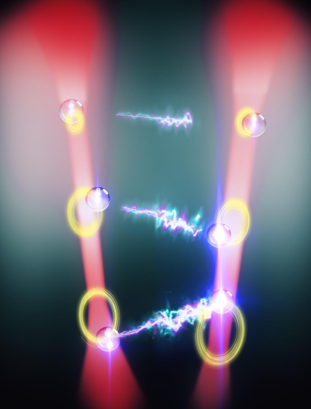
As we transition to a new era in computing, there is a need for new devices that integrate electronic and photonic functionalities at the nanoscale while enhancing the interaction between photons and electrons. In an important step toward fulfilling this need, researchers have developed a new III-V semiconductor nanocavity that confines light at levels below the so-called diffraction limit.

“Nanocavities with ultrasmall mode volumes hold great promise for improving a wide range of photonic devices and technologies, from lasers and LEDs to quantum communication and sensing, while also opening up possibilities in emerging fields such as quantum computing,” said the leading author Meng Xiong from the Technical University of Denmark. “For example, light sources based on these nanocavities could significantly improve communication by enabling faster data transmission and strongly reduced energy consumption.

Page 50 of 313First4748495051525354Last