Menu

Blog

Archive for the ‘nanotechnology’ category: Page 17

Jun 27, 2024

Time-compression in electron microscopy: Terahertz light controls and characterizes electrons in space and time

Posted by in categories: nanotechnology, particle physics, quantum physics

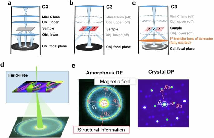
Scientists at the University of Konstanz in Germany have advanced ultrafast electron microscopy to unprecedented time resolution. Reporting in Science Advances, the research team presents a method for the all-optical control, compression, and characterization of electron pulses within a transmission electron microscope using terahertz light. Additionally, the researchers have discovered substantial anti-correlations in the time domain for two-electron and three-electron states, providing deeper insight into the quantum physics of free electrons.

Ultrafast electron microscopy is a cutting-edge technique that combines the spatial resolution of traditional electron microscopy with the of ultrafast femtosecond laser pulses. This powerful combination allows researchers to observe atoms and electrons in motion, capturing dynamic processes in materials with unparalleled clarity. By visualizing these rapid events in space and time, scientists can gain deeper insights into the fundamental mechanisms that govern and transitions, helping to create advancements in research fields such as nanotechnology, optics, materials science, and .

Although ultrafast electron microscopy enables, in principle, the observation of atomic and electronic motions on fundamental spatial and temporal scales, capturing these rapid dynamics has remained challenging due to the limitations in electron pulse duration. The current standard electron pulses, lasting about 200 femtoseconds, are too long to resolve many fundamental reaction processes in materials and molecules. Pulses ten times shorter would be required to observe basic reaction paths and collective atomic motions, so-called phonon modes, in real time.

Jun 27, 2024

Quantum Leap: Ultrafast Light Unlocks New Properties in Low-Dimensional Materials

Posted by in categories: nanotechnology, particle physics

Researchers have identified new characteristics of layered low-dimensional materials that enable rapid transfers of electrons and thermal energy, pointing to potential improvements in ultrafast optical technologies and various other applications.

In a collaborative work in the Dynacom framework (French Japanese Laboratory), recent studies have highlighted that materials composed of layered tubes, which are atomically thick and classified as low-dimensional materials, exhibit new properties. Although the static properties of these structures, such as electrical conduction, are well documented, their dynamic properties, including electron transfer between layers and atomic motion triggered by light exposure, have received less attention.

In this study, scientists constructed nested cylindrical structures by wrapping carbon nanotubes (CNTs) in boron nitride nanotubes. They then examined the motion of electrons and atoms induced by ultrashort light pulses on a one-dimensional (1D) material. Electron motion was monitored using broadband ultrafast optical spectroscopy, which captures instantaneous changes in molecular and electronic structures due to light irradiation with a precision of ten trillionths of a second (10−13 s). Atomic motion was observed through ultrafast time-resolved electron diffraction, which similarly achieved monitoring of structural dynamics with ten-trillionth-of-a-second accuracy.

Jun 26, 2024

Engineers create world’s thinnest wire stable at 0 Kelvin

Posted by in categories: materials, nanotechnology

The team wondered if they could somehow leverage crystalline structures to identify a perfect candidate, sans building thousands of them in a lab.

The researchers were mostly on the lookout for 3D crystals with the right structural and electronic properties, so they could be “exfoliated.” 2D materials like graphene were extracted using this process from 3D.

Continue reading “Engineers create world’s thinnest wire stable at 0 Kelvin” »

Jun 25, 2024

Low power nanoscale S-FED based single ended sense amplifier applied in integrate and fire neuron circuit

Posted by in categories: nanotechnology, neuroscience

Motaman, S., Ghafouri, T. & Manavizadeh, N. Sci Rep 14, 10,691 (2024). https://doi.org/10.1038/s41598-024-61224-x.

Download citation.

Jun 25, 2024

New organoid culture method can verify human toxicity of nanomaterials

Posted by in categories: biotech/medical, nanotechnology

The organoids were treated with zinc oxide nanoparticles (ZnO NPs), which are a liver toxic material, and nontoxic gold nanoparticles (AuNPs). The comparison showed that the toxicity of each material could be accurately observed, in contrast to the conventional method.

Ahruem Baek, a senior researcher at KRISS, said, “Based on our results, we will establish standard nanomaterial and nanomedicine safety assessment procedures using organoids, contributing to the advancement of Korea’s nano-industry.”

The results from this study may allow for rapid and accurate safety assessment of nanomaterials and nanomedicine using organoids, contributing to the safe utilization of nanomaterials in various strategic technical fields.

Jun 25, 2024

Neuromorphic nanoelectronic materials

Posted by in categories: biological, chemistry, nanotechnology, quantum physics, robotics/AI

Memristive and nanoionic devices have recently emerged as leading candidates for neuromorphic computing architectures. While top-down fabrication based on conventional bulk materials has enabled many early neuromorphic devices and circuits, bottom-up approaches based on low-dimensional nanomaterials have shown novel device functionality that often better mimics a biological neuron. In addition, the chemical, structural and compositional tunability of low-dimensional nanomaterials coupled with the permutational flexibility enabled by van der Waals heterostructures offers significant opportunities for artificial neural networks. In this Review, we present a critical survey of emerging neuromorphic devices and architectures enabled by quantum dots, metal nanoparticles, polymers, nanotubes, nanowires, two-dimensional layered materials and van der Waals heterojunctions with a particular emphasis on bio-inspired device responses that are uniquely enabled by low-dimensional topology, quantum confinement and interfaces. We also provide a forward-looking perspective on the opportunities and challenges of neuromorphic nanoelectronic materials in comparison with more mature technologies based on traditional bulk electronic materials.

Jun 23, 2024

Researchers fabricate eco-friendly pesticide delivery system

Posted by in category: nanotechnology

A research team led by Prof. Wu Zhengyan and Zhang Jia from the Hefei Institutes of Physical Science of the Chinese Academy of Sciences has developed a new environmentally friendly way to deliver pesticides using porous microspheres made of halloysite nanotubes (HNTs).

Jun 22, 2024

Advances in nanoscale force measurement opens doors to unprecedented biological insights

Posted by in categories: biological, nanotechnology

New research has revealed a new way to measure incredibly minute forces at the nanoscale in water, pushing the boundaries of what scientists know about the microscopic world.

Jun 21, 2024

Novel Dry Deposition Revolutionizes Carbon Nanotubes

Posted by in categories: computing, nanotechnology

In today’s semiconductor manufacturing industry, the most advanced chips are produced at 7 nm and below where there is little room for error. Despite the difficulty and unrelenting pressures found in this microworld, engineers and scientists remain undeterred in their pursuit of cutting-edge processes, techniques or materials that push the boundaries of Moore’s Law. Through endless experimentation at the nanoscale level, designers and researchers seek to uncover minute improvements that have the potential to translate into millions—if not billions—of dollars in revenue for chipmakers.

The emergence of carbon nanotubes (CNTs) as a compelling alternative material to address inefficiencies in extreme ultraviolet (EUV) lithography has the potential to be one of those innovations. However, contemporary production methods create CNTs that fall short of expectations. To realize the full potential of CNTs requires a new production method that significantly improves their quality. Only then can they help the semiconductor industry deliver on the insatiable demands for advanced chips.

Before exploring the production methods behind creating CNTs, one must first understand why they are so crucial in the semiconductor industry.

Jun 21, 2024

Nanotechnology: How Nanomaterials Are Changing the Game

Posted by in categories: biotech/medical, chemistry, health, nanotechnology, robotics/AI

A series of advances in materials and design have enabled manufacturers to work at scales smaller than a billionth of a size to create devices and objects of nanoscopic dimensions. This is nanotechnology, which, although relatively new, produces materials and technologies already used in mass production.

The European Commission defines nano as any material that is at least 50% composed of particles between one and one hundred nanometers in size (i.e. one billionth of a meter, or one-millionth of a millimeter). Nanomaterials differ from conventional materials because of their unique properties such as higher electrical conductivity and mechanical strength, sensor technologies, and biomedical applications, and because they can create coatings that make surfaces more hydrophobic or self-cleaning.

The widespread use of nanotechnology is relatively new. Since 2000, nanomaterials have been used industrially as new research and experimental designs have made their effectiveness in different sectors clear. For example, in the health field, nanotechnology helps to reduce diagnostic errors and to develop nanobots (microscale robots) to repair and replace intercellular structures, or repair DNA molecules; in the chemical sector, it facilitates coating devices with nanoparticles to improve their smoothness and heat resistance; in manufacturing, materials developed with nanotechnology enhance the performance of the final product by improving heat resistance, strength, durability, and electrical conductivity.

Page 17 of 304First1415161718192021Last