Toggle light / dark theme

Ray Kurzweil is an author, computer scientist, inventor, futurist and a director of engineering at Google. Kurzweil is a public advocate for the futurist and transhumanist movements, and gives public talks to share his optimistic outlook on life extension technologies and the future of nanotechnology, robotics, and biotechnology.

Recorded 2013

The field of epidermal electronics, or e-tattoos, covers a wide range of flexible and stretchable monitoring gadgets that are wearable directly on the skin. We have covered this area in multiple Nanowerk Spotlights, for instance stick-on epidermal electronics tattoo to measure UV exposure or tattoo-type biosensors based on graphene; and we also have posted a primer on electronic skin.

Taking the concept of e-tattoos a step further, integrating them with triboelectric nanogenerators (TENGs), for instance for health monitoring, could lead to next generation wearable nanogenerators and Internet-of-things devices worn directly on and powered by the skin.

In work reported in Advanced Functional Materials (“Triboelectric Nanogenerator Tattoos Enabled by Epidermal Electronic Technologies”), researchers report a tattoo-like TENG (TL-TENG) design with a thickness of tens of micrometers, that can interface with skin without additional adhesive layers, and be used for energy harvesting from daily activities.

Year 2019 😁


Semiconducting carbon nanotubes (CNTs) printed into thin films offer high electrical performance, significant mechanical stability, and compatibility with low-temperature processing. Yet, the implementation of low-temperature printed devices, such as CNT thin-film transistors (CNT-TFTs), has been hindered by relatively high process temperature requirements imposed by other device layers—dielectrics and contacts. In this work, we overcome temperature constraints and demonstrate 1D–2D thin-film transistors (1D–2D TFTs) in a low-temperature (maximum exposure ≤80 °C) full print-in-place process (i.e., no substrate removal from printer throughout the entire process) using an aerosol jet printer. Semiconducting 1D CNT channels are used with a 2D hexagonal boron nitride (h-BN) gate dielectric and traces of silver nanowires as the conductive electrodes, all deposited using the same printer.

Conventional light sources for fiber-optic telecommunications emit many photons at the same time. Photons are particles of light that move as waves. In today €™s telecommunication networks, information is transmitted by modulating the properties of light waves traveling in optical fibers, similar to how radio waves are modulated in AM and FM channels.

In quantum communication, however, information is encoded in the phase of a single photon – the photon €™s position in the wave in which it travels. This makes it possible to connect quantum sensors in a network spanning great distances and to connect quantum computers together.

Researchers recently produced single-photon sources with operating wavelengths compatible with existing fiber communication networks. They did so by placing molybdenum ditelluride semiconductor layers just atoms thick on top of an array of nano-size pillars (Nature Communications, “Site-Controlled Telecom-Wavelength Single-Photon Emitters in Atomically-thin MoTe 2 ”).

Scientists at Scripps Research have reported success in initial tests of a new, nanotech-based strategy against autoimmune diseases.

The scientists, who reported their results in ACS Nano, engineered cell-like “” that target only the driving an autoimmune reaction, leaving the rest of the immune system intact and healthy. The nanoparticles greatly delayed, and in some animals even prevented, in a mouse model of arthritis.

“The potential advantage of this approach is that it would enable safe, long-term treatment for where the immune system attacks its own tissues or organs—using a method that won’t cause broad immune suppression, as current treatments do,” says study senior author James Paulson, Ph.D., Cecil H. and Ida M. Green Chair of Chemistry in the Department of Molecular Medicine at Scripps Research.

The solution to our carbon problem is floating in the oceans.

Phytoplankton are microscopic organisms (can be bacteria, algae, or plants) that perform photosynthesis in oceans and eliminate excess carbon dioxide from Earth’s atmosphere. They sequester about 40 percent of the total carbon produced every year globally and, therefore, also play a major role in mitigating global warming.

A team of researchers from the Pacific Northwest National Laboratory (PNNL) has proposed that by feeding engineered nanoparticles (ENPs) as fertilizers to phytoplankton. Humans can increase the growth of these microorganisms in oceans and eventually fix more CO2 from Earth than ever.

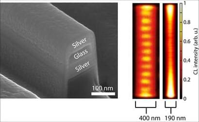
Until recently, physicists widely believed that it was impossible to compress light below the so-called diffraction limit, except when utilizing metal nanoparticles, which also absorb light. As a result, it seemed to be impossible to compress light strongly in dielectric materials like silicon, which are essential for information technologies and had the significant advantage of not absorbing light. Interestingly, it was theoretically shown that the diffraction limit does not apply to dielectrics back in 2006. However, no one has been able to demonstrate this in the actual world due to the fact that it requires such complex nanotechnology that no one has yet been able to create the required dielectric nanostructures.

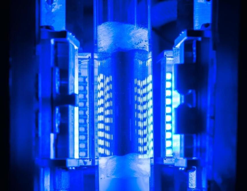
A research team from the Technical University of Denmark has created a device known as a “dielectric nanocavity” that successfully concentrates light in a volume 12 times smaller than the diffraction limit. The finding is groundbreaking in optical research and was recently published in the journal Nature Communications.

Nature Communications is a peer-reviewed, open access, multidisciplinary, scientific journal published by Nature Research. It covers the natural sciences, including physics, biology, chemistry, medicine, and earth sciences. It began publishing in 2010 and has editorial offices in London, Berlin, New York City, and Shanghai.

When charged particles are shot through ultra-thin layers of material, sometimes spectacular micro-explosions occur, and sometimes the material remains almost intact. The reasons for this have now been explained by researchers at the TU Wien.

It sounds a bit like a : Some materials can be shot through with fast, electrically charged ions without exhibiting holes afterwards. What would be impossible at the macroscopic level is allowed at the level of individual particles. However, not all materials behave the same in such situations—in recent years, different research groups have conducted experiments with very different results.

At the TU Wien (Vienna, Austria), it has now been possible to find a detailed explanation of why some materials are perforated and others are not. This is interesting, for example, for the processing of thin membranes, which are supposed to have tailor-made nano-pores in order to trap, hold or let through very specific atoms or molecules there.

A key light-activated nanomaterial for the hydrogen economy has been engineered by researchers at Rice University. Using only inexpensive raw materials, scientists created a scalable catalyst that needs only the power of light to convert ammonia into clean-burning hydrogen fuel.

“This discovery paves the way for sustainable, low-cost hydrogen that could be produced locally rather than in massive centralized plants.” —

The research, which was published on November 24 in the journal Science, was conducted by a team from Rice’s Laboratory for Nanophotonics, Syzygy Plasmonics Inc., and Princeton University.