Menu

Blog

Archive for the ‘nanotechnology’ category: Page 73

Jul 29, 2023

Light enhancement in nanoscale structures could aid cancer detection

Posted by in categories: biotech/medical, nanotechnology

A cutting-edge practice by two Vanderbilt researchers that enhances light in nanoscale structures could help in the detection of diseases like cancer.

The work by Justus Ndukaife, assistant professor of electrical engineering, and Sen Yang, a recent Ph.D. graduate from Ndukaife’s lab in Interdisciplinary Materials Science under Ndukaife, was published in Light: Science & Applications.

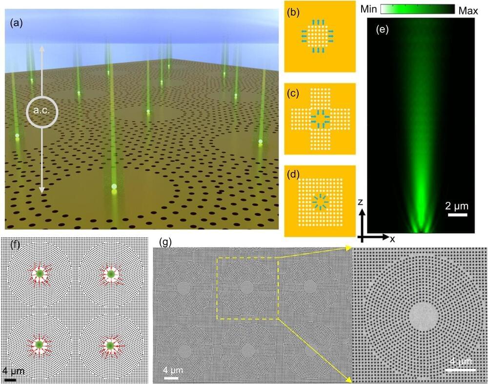
In their paper, they show how an engineered nanostructured surface—quasi-BIC dielectric metasurface—can be used to trap micro and sub-micron particles within seconds, which they say helps in the transport of analytes to biosensing surfaces. The metasurface can also serve as a sensor to detect the aggregated particles or molecules, and can be used to enhance fluorescence or Raman signals from the , thereby boosting detection sensitivity, according to the researchers.

Jul 29, 2023

New protein-based nano-switches could lead to faster, more accurate diagnostic tests

Posted by in categories: bioengineering, biotech/medical, nanotechnology

QUT researchers have developed a new approach for designing molecular ON-OFF switches based on proteins which can be used in a multitude of biotechnological, biomedical and bioengineering applications.

The research team demonstrated that this novel approach allows them to design and build faster and more accurate diagnostic tests for detecting diseases, monitoring water quality and detecting environmental pollutants.

Professor Kirill Alexandrov, of the QUT School of Biology and Environmental Science, lead scientist on the CSIRO-QUT Synthetic Biology Alliance and a researcher with the ARC Centre of Excellence in Synthetic Biology, said that the new technique published in the prestigious scientific journal Nature Nanotechnology demonstrated that protein switches could be engineered in a predictable way.

Jul 28, 2023

Retina cells cultured on nanofiber scaffolds could help treat blindness

Posted by in categories: life extension, nanotechnology, neuroscience

Scientists have found a way to use nanotechnology to create a 3D “scaffold” to grow cells from the retina—paving the way for potential new ways of treating a common cause of blindness.

Researchers, led by Professor Barbara Pierscionek from Anglia Ruskin University (ARU), have been working on a way to successfully grow epithelial (RPE) cells that stay healthy and viable for up to 150 days. RPE cells sit just outside the neural part of the retina, and when damaged, can cause vision to deteriorate. Their work is published in Materials & Design.

It is the first time this technology, called “electrospinning,” has been used to create a scaffold on which the RPE cells could grow, and could revolutionize treatment for one of age-related macular degeneration, one of the world’s most common vision complaints.

Jul 27, 2023

Researchers demonstrate scaling of aligned carbon nanotube transistors to below sub-10 nm nodes

Posted by in categories: computing, nanotechnology, particle physics

Carbon nanotubes, large cylindrical molecules composed of hybridized carbon atoms arranged in a hexagonal structure, recently attracted significant attention among electronics engineers. Due to their geometric configuration and advantageous electronic properties, these unique molecules could be used to create smaller field-effect transistors (FETs) that exhibit high energy efficiencies.

FETs based on carbon nanotubes have the potential to outperform smaller transistors based on silicon, yet their advantage in real-world implementations has yet to be conclusively demonstrated. A recent paper by researchers at Peking University and other institutes in China, published in Nature Electronics, outlines the realization of FETs based on carbon nanotubes that can be scaled to the same size of a 10 nm silicon technology node.

“Recent progress in achieving wafer-scale high density semiconducting carbon nanotube arrays brough us one step closer to the practical use of carbon nanotubes in CMOS circuits,” Zhiyong Zhang, one of the researchers who carried out the study, told Phys.org. “However, previous research efforts have mainly focused on the scaling of channel or gate length of carbon nanotube transistors while keeping large contact dimensions, which cannot be accepted for high density CMOS circuits in practical applications.

Jul 26, 2023

New study reveals spin in quantum dots’ carrier multiplication

Posted by in categories: chemistry, nanotechnology, quantum physics, solar power, sustainability

A new approach to developing semiconductor materials at tiny scales could help boost applications that rely on converting light to energy. A Los Alamos-led research team incorporated magnetic dopants into specially engineered colloidal quantum dots—nanoscale-size semiconductor crystals—and was able to achieve effects that may power solar cell technology, photo detectors and applications that depend on light to drive chemical reactions.

“In quantum dots comprising a lead-selenide core and a cadmium-selenide shell, manganese ions act as tiny magnets whose magnetic spins strongly interact with both the core and the shell of the quantum dot,” said Victor Klimov, leader of the Los Alamos nanotechnology team and the project’s principal investigator. “In the course of these interactions, energy can be transferred to and from the manganese ion by flipping its spin—a process commonly termed spin exchange.”

In spin-exchange multiplication, a single absorbed photon generates not one but two , also known as excitons, which occur as a result of spin-flip relaxation of an excited manganese ion.

Jul 26, 2023

Research team develops a washable, transparent, and flexible OLED with MXene nanotechnology

Posted by in categories: computing, health, military, nanotechnology

Transparent and flexible displays, which have received a lot of attention in various fields including automobile displays, bio–health care, military, and fashion, are in fact known to break easily when experiencing small deformations. To solve this problem, active research is being conducted on many transparent and flexible conductive materials such as carbon nanotubes, graphene, silver nanowires, and conductive polymers.

A joint research team led by Professor Kyung Cheol Choi from the KAIST School of Electrical Engineering and Dr. Yonghee Lee from the National Nano Fab Center (NNFC) announced the successful development of a water-resistant, transparent, and flexible OLED using MXene nanotechnology. The material can emit and transmit light even when exposed to water.

This research was published as a front cover story of ACS Nano under the title “Highly Air-Stable, Flexible, and Water-Resistive 2D Titanium Carbide MXene-Based RGB Organic Light-Emitting Diode Displays for Transparent Free-Form Electronics.”

Jul 25, 2023

A new type of quantum bit in semiconductor nanostructures

Posted by in categories: computing, nanotechnology, quantum physics

Researchers have created a quantum superposition state in a semiconductor nanostructure that might serve as a basis for quantum computing. The trick: two optical laser pulses that act as a single terahertz laser pulse.

A German-Chinese research team has successfully created a quantum bit in a semiconductor nanostructure. Using a special energy transition, the researchers created a state in a quantum dot—a tiny area of the semiconductor—in which an electron hole simultaneously possessed two different energy levels. Such superposition states are fundamental for quantum computing.

However, excitation of the state would require a large-scale free-electron that can emit light in the terahertz range. Additionally, this wavelength is too long to focus the beam on the tiny quantum dot. The German-Chinese team has now achieved the excitation with two finely tuned short-wavelength optical .

Jul 25, 2023

Breaking barriers in drug delivery with better lipid nanoparticles

Posted by in categories: biotech/medical, nanotechnology

Many diseases can be successfully treated in the simple environment of a cell culture dish, but to successfully treat real people, the drug agent has to take a journey through the infinitely more complex environment within our bodies and arrive, intact, inside the affected cells. This process, called drug delivery, is one of the most significant barriers in medicine.

A collaboration between Lawrence Berkeley National Laboratory (Berkeley Lab) and Genentech, a member of the Roche Group, is working to break through some of the bottlenecks by designing the most effective lipid nanoparticles (LNPs)—tiny spherical pouches made of fatty molecules that encapsulate therapeutic agents until they dock with cell membranes and release their contents. The first drug to use LNPs was approved in 2018, but the delivery method rose to global prominence with the Pfizer and Moderna mRNA COVID vaccines.

“It’s quite a smart system, because if you just deliver the RNA itself to the human body, the RNA is degraded by nucleases and cannot easily cross the cell membrane due to its size and charge, but the LNPs deliver it safely into the cell,” explained co-lead author Chun-Wan Yen, a senior Principal Scientist in Genentech’s Small Molecule Pharmaceutical Sciences group.

Jul 24, 2023

Robot made of LEGOs produces DNA machines

Posted by in categories: bioengineering, biotech/medical, nanotechnology, robotics/AI

A team of ingenious bioengineers at Arizona State University (ASU) has harnessed the power of childhood nostalgia, unveiling a creative solution to a long-standing challenge in DNA origami research.

They’ve successfully employed a LEGO robotics kit to build an affordable, highly effective gradient mixer for purifying self-assembling DNA origami nanostructures. This innovative breakthrough, detailed in a paper published one PLOS ONE, promises to revolutionize how scientists approach DNA origami synthesis.

The creation of DNA origami structures is an intricate process, requiring precise purification of nanostructures. Traditionally, this purification step involved rate-zone centrifugation, relying on a costly piece of equipment called a gradient mixer. However, the maverick minds at ASU have demonstrated that even the iconic plastic bricks of LEGO can be repurposed for scientific advancement.

Jul 24, 2023

Shrinking light: Waveguiding scheme enables highly confined subnanometer optical fields

Posted by in categories: nanotechnology, quantum physics

Imagine shrinking light down to the size of a tiny water molecule, unlocking a world of quantum possibilities. This has been a long-held dream in the realms of light science and technology. Recent advancements have brought us closer to achieving this incredible feat, as researchers from Zhejiang University have made groundbreaking progress in confining light to subnanometer scales.

Traditionally, there have been two approaches to localize light beyond its typical diffraction limit: dielectric confinement and plasmonic confinement. However, challenges such as precision fabrication and optical loss have hindered the confinement of optical fields to sub-10 nanometer (nm) or even 1-nm levels. But now, a new waveguiding scheme reported in Advanced Photonics promises to unlock the potential of subnanometer optical fields.

Picture this: Light travels from a regular , embarking on a transformative journey through a fiber taper, and finds its destination in a coupled-nanowire-pair (CNP). Within the CNP, the light morphs into a remarkable nano-slit mode, generating a confined optical field that can be as tiny as a mere fraction of a nanometer (approximately 0.3 nm). With an astonishing efficiency of up to 95% and a high peak-to-background ratio, this novel approach offers a whole new world of possibilities.

Page 73 of 304First7071727374757677Last