Menu

Blog

Archive for the ‘nanotechnology’ category: Page 15

Jul 10, 2024

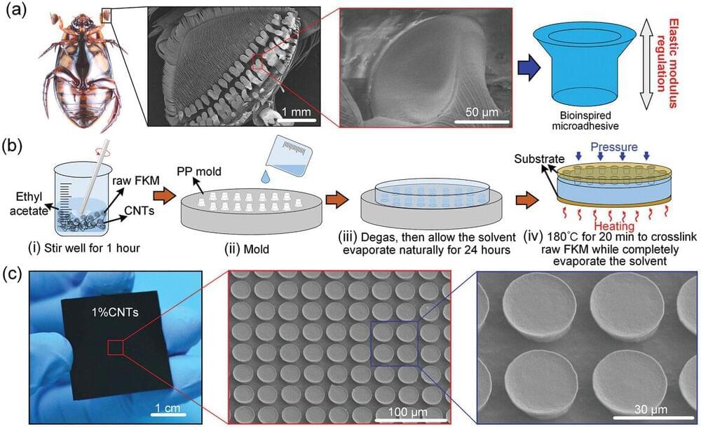
Flexible nanoimprint lithography enables efficient fabrication of biomimetic microstructures

Posted by in categories: augmented reality, computing, nanotechnology, sustainability, virtual reality

Gallium nitride (GaN)-based light-emitting diodes (LEDs) have transformed the lighting industry by replacing conventional lighting technologies with superior energy efficiency, longer operating life and greater environmental sustainability.

In recent years, considerable attention has been paid to the trend toward miniaturization of LEDs, driven by display devices, augmented reality, virtual reality, and other emerging technologies. Due to the lack of cost-effective native substrates, the presence of high threading dislocation density in heteroepitaxial films grown on sapphire substrate is a major limiting factor for device performance.

In addition, Fresnel reflections at the interface between epitaxy and substrate caused by abrupt changes in the refractive indices of the material reduce the light energy utilization.

Jul 8, 2024

Google’s AI visionary says we’ll ‘expand intelligence a millionfold by 2045’ thanks to nanobots, the tech will resurrect the dead, and we’re all going to live forever

Posted by in categories: life extension, nanotechnology, robotics/AI

Forget a pinch of salt, this guy’s predictions need the full shaker.

Jul 7, 2024

Researchers explain the imaging mechanisms of atomic force microscopy in 3D

Posted by in categories: biological, nanotechnology, transportation

Researchers at Nano Life Science Institute (WPI-NanoLSI), Kanazawa University report the 3D imaging of a suspended nanostructure. The technique used is an extension of atomic force microscopy and is a promising approach for visualizing various 3D biological systems.

Atomic force microscopy (AFM) was originally invented for visualizing surfaces with nanoscale resolution. Its basic working principle is to move an ultrathin tip over a sample’s surface. During this xy-scanning motion, the tip’s position in the direction perpendicular to the xy-plane follows the sample’s height profile, resulting in a height map of the surface.

In recent years, ways to extend the method to 3D imaging have been explored, with researchers from Nano Life Science Institute (WPI-NanoLSI), Kanazawa University reporting pioneering experiments on living cells. However, for 3D-AFM to evolve into a widely applicable technique for visualizing flexible molecular structures, a thorough understanding of the imaging mechanisms at play is necessary.

Jul 7, 2024

Research team creates process to grow sub-nanometer transistors

Posted by in categories: computing, nanotechnology, quantum physics, space

Why it matters: Moore’s Law might not be dead after all. A new technique using nanomaterials can further miniaturize transistors, allowing fab plants to pack more of them on each chip. This research opens up new possibilities for creating advanced semiconductor devices with features smaller than current lithography techniques allow.

A South Korean research team led by Director Jo Moon-Ho of the Center for Van der Waals Quantum Solids within South Korea’s Institute for Basic Science has made a significant advancement in semiconductor and nanomaterial technology that could lead to the development of much smaller, more efficient, and more powerful electronic devices. The new technique can grow “one-dimentional” metallic nanaomaterials with widths as narrow as 0.4 nanometers for use as gate electrodes on 2D substrates. The technique promises to overcome the limitations of traditional lithography.

Integrated devices based on two-dimensional semiconductors exhibit excellent electrical properties even when thinned to atomic-scale thickness, making them promising candidates for creating ultra-thin, high-performance electronic devices. A separate study indicates that these 2D logic circuits are promising candidates for the post-Moore’s Law era.

Jul 6, 2024

Sound Science: How Phononic Crystals are Shaping Quantum Computing

Posted by in categories: computing, genetics, information science, mobile phones, nanotechnology, quantum physics, science

Researchers have developed a genetic algorithm for designing phononic crystal nanostructures, significantly advancing quantum computing and communications.

The new method, validated through experiments, allows precise control of acoustic wave propagation, promising improvements in devices like smartphones and quantum computers.

Quantum Computing Revolution

Jul 6, 2024

A 2D Device May Help Quantum Computers Stay Cool

Posted by in categories: computing, nanotechnology, quantum physics

PRESS RELEASE — To perform quantum computations, quantum bits (qubits) must be cooled down to temperatures in the millikelvin range (close to-273 Celsius), to slow down atomic motion and minimize noise. However, the electronics used to manage these quantum circuits generate heat, which is difficult to remove at such low temperatures. Most current technologies must therefore separate quantum circuits from their electronic components, causing noise and inefficiencies that hinder the realization of larger quantum systems beyond the lab.

Researchers in EPFL’s Laboratory of Nanoscale Electronics and Structures (LANES), led by Andras Kis, in the School of Engineering have now fabricated a device that not only operates at extremely low temperatures, but does so with efficiency comparable to current technologies at room temperature.

Jul 5, 2024

Getting bacteria into line: Physicists use magnetic fields to manipulate bacterial behavior

Posted by in categories: nanotechnology, physics

Researchers at Finland’s Aalto University have found a way to use magnets to line up bacteria as they swim. The approach offers more than just a way to nudge bacteria into order—it also provides a useful tool for a wide range of research, such as work on complex materials, phase transitions and condensed matter physics.

The paper is published in the journal Communications Physics.

Bacterial cells generally aren’t magnetic, so the magnets don’t directly interact with the bacteria. Instead, the bacteria are mixed into a liquid with millions of . This means the rod-shaped bacteria are effectively non-magnetic voids inside the magnetic fluid.

Jul 4, 2024

Researchers Achieve High Vacuum Levitation of Silica Nanoparticle, Paving the Way for Future Levitation Technologies

Posted by in categories: computing, nanotechnology

Researchers achieved high-vacuum levitation of a silica nanoparticle on a photonic-electric chip, revolutionizing nanotechnology.

Jul 3, 2024

Scientists discover way to ‘grow’ sub-nanometer sized transistors

Posted by in categories: computing, nanotechnology, quantum physics, space

A research team led by Director Jo Moon-Ho of the Center for Van der Waals Quantum Solids within the Institute for Basic Science (IBS) has implemented a novel method to achieve epitaxial growth of 1D metallic materials with a width of less than 1 nm. The group applied this process to develop a new structure for 2D semiconductor logic circuits. Notably, they used the 1D metals as a gate electrode of the ultra-miniaturized transistor.

This research appears in Nature Nanotechnology.

Integrated devices based on two-dimensional (2D) semiconductors, which exhibit excellent properties even at the ultimate limit of material thickness down to the atomic scale, are a major focus of basic and applied research worldwide. However, realizing such ultra-miniaturized transistor devices that can control the electron movement within a few nanometers, let alone developing the manufacturing process for these integrated circuits, has been met with significant technical challenges.

Jul 3, 2024

Researchers discover way to ‘grow’ sub-nanometer sized transistors

Posted by in categories: computing, nanotechnology, quantum physics, space

A research team led by Director JO Moon-Ho of the Center for Van der Waals Quantum Solids within the Institute for Basic Science (IBS) has implemented a novel method to achieve epitaxial growth of 1D metallic materials with a width of less than 1 nanometer (nm). The group applied this process to develop a new structure for 2D semiconductor logic circuits. Notably, they used the 1D metals as a gate electrode of the ultra-miniaturized transistor.

This research was published in the journal Nature Nanotechnology (“Integrated 1D epitaxial mirror twin boundaries for ultra-scaled 2D MoS 2 field-effect transistors”).

Integrated devices based on two-dimensional (2D) semiconductors, which exhibit excellent properties even at the ultimate limit of material thickness down to the atomic scale, are a major focus of basic and applied research worldwide. However, realizing such ultra-miniaturized transistor devices that can control the electron movement within a few nanometers, let alone developing the manufacturing process for these integrated circuits, has been met with significant technical challenges.

Page 15 of 304First1213141516171819Last