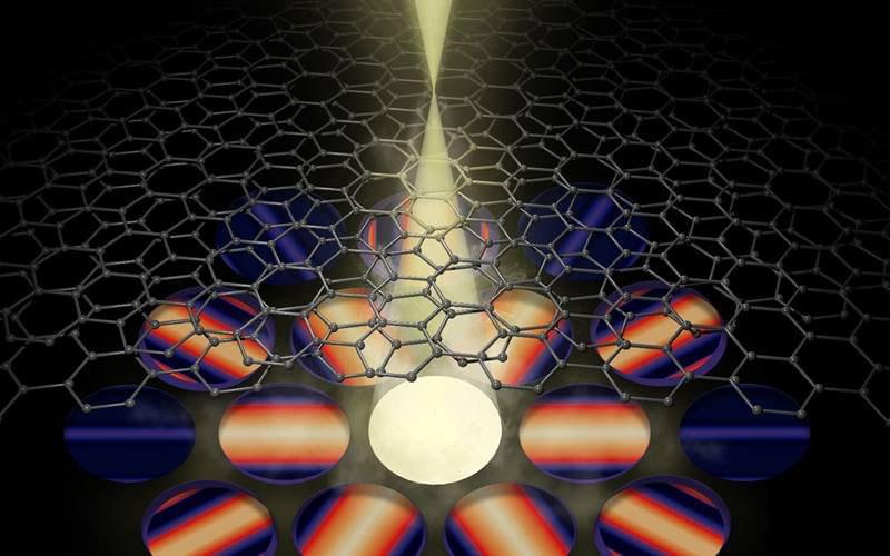
Two-dimensional (2D) materials, composed of a single or a few layers of atoms, are at the forefront of material science, promising revolutionary advancements in technology. These ultra-thin materials exhibit unique and exotic properties, particularly when their layers are stacked and twisted in specific ways.
This manipulation of layers can significantly alter their electronic characteristics, presenting exciting opportunities for the development of next-generation technologies such as more efficient computers and reliable electricity storage systems.
Understanding the intricate relationship between the atomic structure and electronic properties of these materials, however, poses a significant challenge. Traditional microscopy techniques struggle to capture the complete 3D atomic structure of these layered materials, especially when the layers are oriented differently or composed of light elements.


Comments are closed.