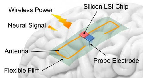
Human and animal movements generate slight neural signals from their brain cells. These signals obtained using a neural interface are essential for realizing brain-machine interfaces (BMI). Such neural recording systems using wires to connect the implanted device to an external device can cause infections through the opening in the skull. One method of solving this issue is to develop a wireless neural interface that is fully implantable on the brain.
However, the neural interface implanted on the brain surface should be of small size and minimally invasive. Furthermore, it requires the integration of a power source, antenna for wireless communication, and many functional circuits.
Now, a research team at the Department of Electrical and Electronic Information Engineering at Toyohashi University of Technology has developed a wafer-level packaging technique to integrate a silicon large-scale integration (LSI) chip in a very thin film of a thickness 10 µm (Sensors, “Co-design method and wafer-level packaging technique of thin-film flexible antenna and silicon CMOS rectifier chips for wireless-powered neural interface systems”).


Comments are closed.