If scientists could find a way to control the process for making semiconductor components on a nanometric scale, they could give those components unique electronic and optical properties—opening the door to a host of useful applications.
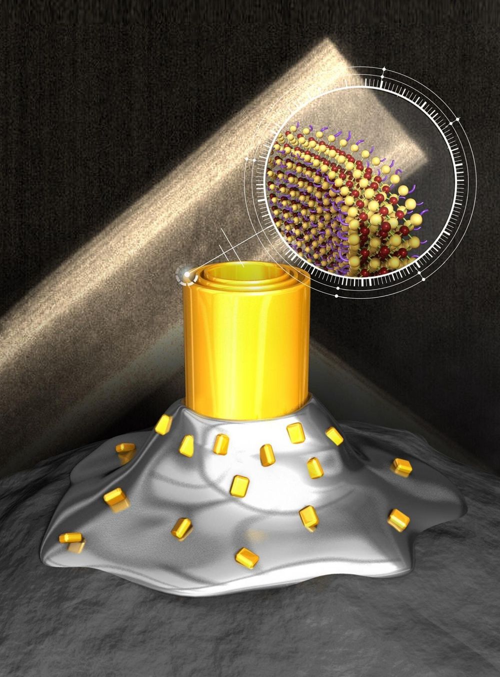
Researchers at the Laboratory of Microsystems, in EPFL’s School of Engineering, have taken an important step towards that goal with their discovery of semiconducting nanotubes that assemble automatically in solutions of metallic nanocrystals and certain ligands. The tubes have between three and six walls that are perfectly uniform and just a few atoms thick—making them the first such nanostructures of their kind.
What’s more, the nanotubes possess photoluminescent properties: they can absorb light of a specific wavelength and then send out intense light waves of a different color, much like quantum dots and quantum wells. That means they can be used as fluorescent markers in medical research, for example, or as catalysts in photoreduction reactions, as evidenced by the removal of the colors of some organic dyes, based on the results of initial experiments. The researchers’ findings have made the cover of ACS Central Science.
