Archive for the ‘nanotechnology’ category: Page 284
Jun 9, 2016
Living computers and nano-robots: what’s the future for DNA manipulation?
Posted by Karen Hurst in categories: biotech/medical, computing, nanotechnology, robotics/AI
Jun 9, 2016
Using Adenosine Triphosphate to Create Biological Super-Computers
Posted by Karen Hurst in categories: biotech/medical, computing, engineering, nanotechnology, sustainability
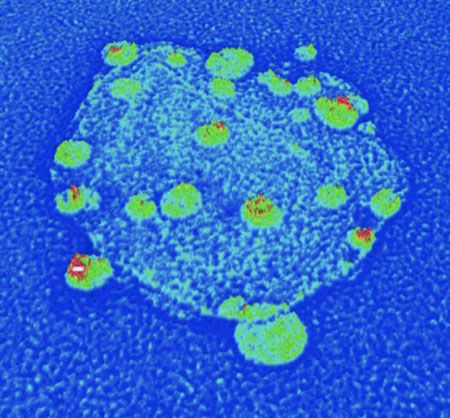
Machines running on human energy? Yes, it can happen, according to Dan Nicolau, Jr. from the Department of Integrative Biology at the University of California. Nicolau and his colleagues successfully completed a proof-of-concept study of a book-sized computer that runs on adenosine triphosphate (ATP), a biochemical that releases energy in cells and aids in energy transfer.
The study results published in the Proceedings of the National Academy of Sciences (PNAS), describe the combination of geometrical modeling and engineering as well as nanotechnology to create circuitry that uses 1.5 × 1.5 cm in area and the naturally occurring protein to operate.
A More Sustainable Option
Continue reading “Using Adenosine Triphosphate to Create Biological Super-Computers” »
Jun 8, 2016
Pairing nanodiamonds with other nanomaterials could enable huge advances in nanotechnology
Posted by Karen Hurst in categories: 3D printing, business, computing, nanotechnology, quantum physics
Very promising. I imagine 3D Printers being able to create synthesize diamonds will be a very profitable business to get in to because of the stabilizing benefits that the nanodiamonds bring to Quantum Computing and nanotechnology in general.
Nanomaterials have the potential to improve many next-generation technologies. They promise to speed up computer chips, increase the resolution of medical imaging devices and make electronics more energy efficient. But imbuing nanomaterials with the right properties can be time consuming and costly. A new, quick and inexpensive method for constructing diamond-based hybrid nanomaterials could soon launch the field forward.
University of Maryland researchers developed a method to build diamond-based hybrid nanoparticles in large quantities from the ground up, thereby circumventing many of the problems with current methods. The technique is described in the June 8, 2016 issue of the journal Nature Communications (“Nanostructures for Coupling Nitrogen-Vacancy Centers to Metal Nanoparticles and Semiconductor Quantum Dots”).
Jun 6, 2016
Meta-lens works in the visible spectrum, sees smaller than a wavelength of light
Posted by Karen Hurst in category: nanotechnology
Curved lenses, like those in cameras or telescopes, are stacked in order to reduce distortions and resolve a clear image. That’s why high-power microscopes are so big and telephoto lenses so long.
While lens technology has come a long way, it is still difficult to make a compact and thin lens (rub a finger over the back of a cellphone and you’ll get a sense of how difficult). But what if you could replace those stacks with a single flat—or planar—lens?
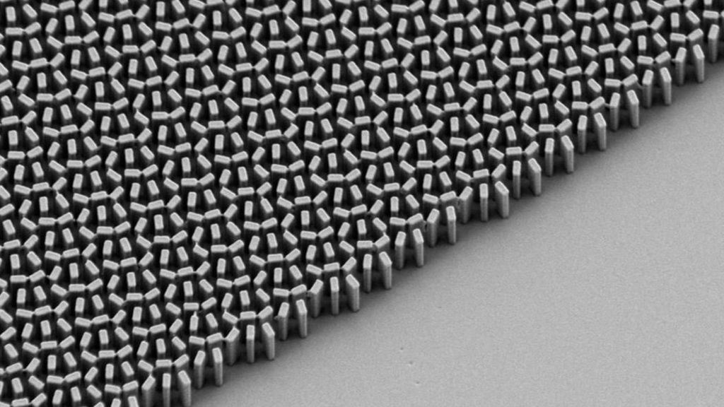
Researchers from the Harvard John A. Paulson School of Engineering and Applied Sciences (SEAS) have demonstrated the first planar lens that works with high efficiency within the visible spectrum of light—covering the whole range of colors from red to blue. The lens can resolve nanoscale features separated by distances smaller than the wavelength of light. It uses an ultrathin array of tiny waveguides, known as a metasurface, which bends light as it passes through, similar to a curved lens.
Jun 6, 2016
Applications of Nanoparticle Tracking Analysis in Nanomedicine
Posted by Karen Hurst in categories: nanotechnology, quantum physics
Since 2001, I have worked, experimented, and researched in parallel tech and bio/medical technology space. I did this because I could see that at some point that these two fields would eventually overlap and eventually merge in many areas. Today, we’re already see the duplicated use of technology in both the medical/ life sciences and the same technology used to advance the technology in general such as Quantum tech, nanotech, etc. Here is another example of this trend.
Sponsored Content by Malvern Instruments Ltd
Introduction
Continue reading “Applications of Nanoparticle Tracking Analysis in Nanomedicine” »
Jun 6, 2016
Tiny lasers on silicon means big things for electronics
Posted by Karen Hurst in categories: computing, electronics, nanotechnology, quantum physics, solar power, sustainability
Silicon forms the basis of everything from solar cells to the integrated circuits at the heart of our modern electronic gadgets. However the laser, one of the most ubiquitous of all electronic devices today, has long been one component unable to be successfully replicated in this material. Now researchers have found a way to create microscopically-small lasers directly from silicon, unlocking the possibilities of direct integration of photonics on silicon and taking a significant step towards light-based computers.
Whilst there has been a range of microminiature lasers incorporated directly into silicon over the years, including melding germanium-tin lasers with a silicon substrate and using gallium-arsenide (GaAs) to grow laser nanowires, these methods have involved compromise. With the new method, though, an international team of researchers has integrated sub-wavelength cavities, the basic components of their minuscule lasers, directly onto the silicon itself.
To help achieve this, a team of collaborating scientists from Hong Kong University of Science and Technology, the University of California, Santa Barbara, Sandia National Laboratories and Harvard University, first had to find a way to refine silicon crystal lattices so that their inherent defects were reduced significantly enough to match the smooth properties found in GaAs substrate lasers. They did this by etching nano-patterns directly onto the silicon to confine the defects and ensure the necessary quantum confinement of electrons within quantum dots grown on this template.
Jun 4, 2016
Flat lens promises possible revolution in optics
Posted by Shailesh Prasad in category: nanotechnology
A flat lens made of paint whitener on a sliver of glass could revolutionise optics, according to its US inventors.
Just 2mm across and finer than a human hair, the tiny device can magnify nanoscale objects and gives a sharper focus than top-end microscope lenses.
It is the latest example of the power of metamaterials, whose novel properties emerge from their structure.
Jun 2, 2016
Tiny lasers enable next-gen microprocessors to run faster, less power-hungry
Posted by Karen Hurst in categories: electronics, energy, nanotechnology
More energy efficient, high performance microprocessors on the way.
Abstract: Tiny high-performance lasers grown directly on silicon wafers solve a decades-old semiconductor industry challenge that, until now, has held back the integration of photonics with electronics on the silicon platform,
A group of scientists from Hong Kong University of Science and Technology; the University of California, Santa Barbara; Sandia National Laboratories and Harvard University were able to fabricate tiny lasers directly on silicon — a huge breakthrough for the semiconductor industry and well beyond.
Continue reading “Tiny lasers enable next-gen microprocessors to run faster, less power-hungry” »
Jun 2, 2016
New nanotech fabric dissolves odor and stains whenever it’s exposed to bright light
Posted by Shailesh Prasad in categories: energy, nanotechnology
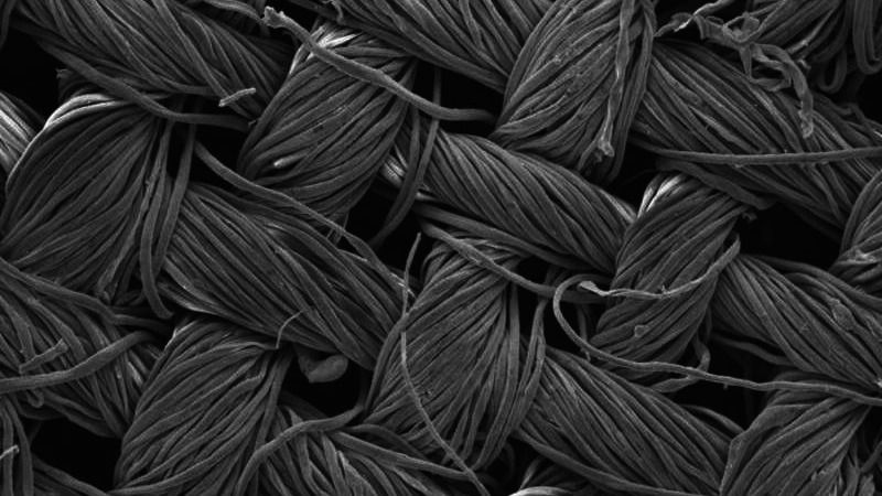
Not a big fan of laundry day? Well what if you could wash your clothes just by stepping into the sunshine? Thanks to researchers at RMIT University in Melbourne, a self-cleaning textile could make that possible in the very near future. With the help of special nanostructures grown directly into the fabric, these new textiles could degrade organic matter like dirt, dust, and sweat when exposed to a concentrated light source.
To achieve this effect, the nanostructures used by the RMIT University team are made copper and silver. These metals are great at absorbing visible light, and when they’re exposed to light from the sun or even a light bulb, the nanostructures react with increased energy that creates “hot electrons”.
Related: Columbia’s most comfortable clothes are also its smartest, thanks to textile tech.


