Menu

Blog

Archive for the ‘engineering’ category: Page 70

Dec 13, 2022

New 3D model shows how the paradise tree snake uses aerial undulation to fly

Posted by in categories: biotech/medical, engineering, mathematics

When the paradise tree snake flies from one tall branch to another, its body ripples with waves like green cursive on a blank pad of blue sky. That movement, aerial undulation, happens in each glide made by members of the Chrysopelea family, the only known limbless vertebrates capable of flight. Scientists have known this, but have yet to fully explain it.

For more than 20 years, Jake Socha, a professor in the Department of Biomedical Engineering and Mechanics at Virginia Tech, has sought to measure and model the biomechanics of snake flight and answer questions about them, like that of aerial undulation’s functional role. For a study published by Nature Physics, Socha assembled an interdisciplinary team to develop the first continuous, anatomically-accurate 3D mathematical model of Chrysopelea paradisi in flight.

The team, which included Shane Ross, a professor in the Kevin T. Crofton Department of Aerospace and Ocean Engineering, and Isaac Yeaton, a recent mechanical engineering doctoral graduate and the paper’s lead author, developed the 3D model after measuring more than 100 live snake glides. The model factors in frequencies of undulating waves, their direction, forces acting on the body, and mass distribution. With it, the researchers have run virtual experiments to investigate aerial undulation.

Dec 13, 2022

Japan’s New Semiconductor Foundry Rapidus Taps IBM For 2nm Process

Posted by in categories: business, computing, engineering, finance, government

Japan wants to get back into the leading-edge semiconductor business and very recently a new company was formed to reboot its semiconductor industry. The company is named Rapidus, referring to rapid production of new chips, a clear reference to how the company plans to differentiate its business from other foundries such as TSMC, Samsung, and Intel. The company has announced a partnership with IBM Research to develop IBM’s 2nm technology in fabs that Rapidus plans to build in Japan during the second part of this decade. Previously, Rapidus announced a collaboration with the Belgium-based microelectronics research hub IMEC on advanced semiconductor technologies. Imec is collaborative semiconductor research organization working the world’s major foundries, IDMs, fabless and fablite companies, material and tool suppliers, EDA companies and application developers.

The IBM process uses gate-all-around transistors — IBM refers to them as nano sheet FETs — which is the next generation of transistor design that enables device scaling beyond today’s FinFETs. The 2nm structures will require Rapidus to use ASML’s EUV manufacturing equipment. Business details with IBM were not disclosed, but there’s likely two parts to the deal: a cross-licensing agreement for the intellectual property necessary to build the product and a joint development agreement. While the announcement is nominally for IBM’s 2nm process, it likely includes a long-term commitment to build advanced semiconductor chips going beyond the 2nm process node.

Rapidus was formed by semiconductor veterans such as Rapidus President Atsuyoshi Koike, with backing by leading Japanese technology and financial firms, including Denso, Kioxia, Mitsubishi UFJ Bank, NEC, NTT, Softbank, Sony, and Toyota Motor. The Japanese government is also subsidizing Rapidus. The big change for Japan compared to prior national efforts is the collaboration with international organizations. It’s a recognition Japan cannot go it alone. This appears to be a fundamental change in Japanese attitudes. Building a fab in Japan will be helped by Japan’s strong manufacturing ecosystem of materials, equipment, and engineering talent.

Dec 11, 2022

How To Terraform Mars — WITH LASERS

Posted by in categories: engineering, environmental, space

Go ‘beyond the nutshell’ at https://brilliant.org/nutshell by diving deeper into these topics and more with 20% off an annual subscription!
This video was sponsored by Brilliant. Thanks a lot for the support!

Sources & further reading:
https://sites.google.com/view/sources-mars-terraforming.

Continue reading “How To Terraform Mars — WITH LASERS” »

Dec 10, 2022

Engineers Push Probabilistic Computing Closer to Reality

Posted by in categories: computing, engineering, information science, quantum physics

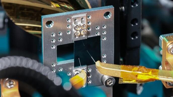
A large universal quantum computer is still an engineering dream, but machines designed to leverage quantum effects to solve specific classes of problems—such as D-wave’s computers—are alive and well. But an unlikely rival could challenge these specialized machines: computers built from purposely noisy parts.

This week at the IEEE International Electron Device Meeting (IEDM 2022), engineers unveiled several advances that bring a large-scale probabilistic computer closer to reality than ever before.

Quantum computers are unrivaled for any algorithm that relies on quantum’s complex amplitudes. “But for problems where the numbers are positive, sometimes called stochastic problems, probabilistic computing could be quite competitive,” says Supriyo Datta, professor of electrical and computer engineering at Purdue University and one of the pioneers of probabilistic computing.

Dec 9, 2022

Quantum light source could pave the way to a quantum internet

Posted by in categories: engineering, internet, quantum physics

The ability to integrate fiber-based quantum information technology into existing optical networks would be a significant step toward applications in quantum communication. To achieve this, quantum light sources must be able to emit single photons with controllable positioning and polarization and at 1.35 and 1.55 micrometer ranges where light travels at minimum loss in existing optical fiber networks, such as telecommunications networks. This combination of features has been elusive until now, despite two decades of research efforts.

Recently, two-dimensional (2D) semiconductors have emerged as a novel platform for next-generation photonics and electronics applications. Although scientists have demonstrated 2D quantum emitters operating at the visible regime, single-photon emission in the most desirable telecom bands has never been achieved in 2D systems.

To solve this problem, researchers at Los Alamos National Laboratory developed a strain engineering protocol to deterministically create two-dimensional quantum light emitters with operating wavelength tunable across O and C telecommunication bands. The polarization of the emissions can be tuned with a magnetic field by harnessing the valley degree of freedom.

Dec 9, 2022

The Megastructure Compendium

Posted by in categories: cosmology, engineering, nanotechnology, nuclear energy, sustainability

Sign up for a Curiosity Stream subscription and also get a free Nebula subscription (the streaming platform built by creators) here: https://curiositystream.com/isaacarthur.
In the future humanity may build enormous structures, feats of mega-engineering that may rival planets or even be of greater scope. This episode catalogs roughly 100 major types of Megastructure, from those that are cities in space to those that rival galaxies.

Visit our Website: http://www.isaacarthur.net.
Support us on Patreon: https://www.patreon.com/IsaacArthur.
Support us on Subscribestar: https://www.subscribestar.com/isaac-arthur.
Facebook Group: https://www.facebook.com/groups/1583992725237264/
Reddit: https://www.reddit.com/r/IsaacArthur/
Twitter: https://twitter.com/Isaac_A_Arthur on Twitter and RT our future content.
SFIA Discord Server: https://discord.gg/53GAShE

Continue reading “The Megastructure Compendium” »

Dec 9, 2022

Researchers harvest electricity from wood soaking in water

Posted by in categories: energy, engineering

Water and wood may one day be all that’s needed to provide electrical power for a household. At a time when energy is a critical issue for many millions of people worldwide, scientists in Sweden have managed to generate electricity with the help of these two renewable resources.

The method reported by researchers at KTH Royal Institute of Technology focuses on what naturally happens after is placed in water, and the water evaporates. Transpiration, a process in which water moves through a plant, is constantly occurring in nature. And it produces small amounts of , known as bioelectricity.

Yuanyuan Li, assistant professor at the Division of Biocomposites at KTH, says that with some nanoengineering of wood—and pH tuning—small but promising amounts of electricity can now be harvested.

Dec 8, 2022

A ‘heart attack on a chip’ device could lead to treatments for cardiovascular disease

Posted by in categories: biotech/medical, engineering, life extension

Researchers use the device to study heart attacks and hope to test new heart medications.

Researchers have developed a device that can mimic aspects of a heart attack with hopes of using the device to test and develop novel heart medications. The research team, from the University of Southern California Alfred E. Mann Department of Biomedical Engineering in the U.S., created the tool, which they call a “heart attack on a chip.”

The study was published in the journal Science Advances.

Continue reading “A ‘heart attack on a chip’ device could lead to treatments for cardiovascular disease” »

Dec 8, 2022

A reconfigurable device based on 2D van der Waals heterostructures that works both as a transistor and memory

Posted by in categories: computing, engineering

One key objective of electronics engineering research is to develop computing devices that are both highly performing and energy-efficient, meaning that they can compute information quickly while consuming little power. One possible way to do this could be to combine units that perform logic operations and memory components into a single device.

So far, most computing devices have been made up of a processing unit and a physically separate component. The creation of a device that can efficiently perform both these functions, referred to as a logic-in-memory architecture, could help to significantly simplify devices and cut down their power consumption.

While a few of the logic-in-memory architectures proposed so far achieved promising results, most existing solutions come with practical limitations. For instance, some devices have been found to be unstable, unreliable or only applicable to specific use cases.

Dec 6, 2022

Chip lets scientists study biocement formation in real-time

Posted by in categories: biotech/medical, computing, engineering, health

Scientists from EPFL and the University of Lausanne have used a chip that was originally designed for environmental science to study the properties of biocement formation. This material has the potential to replace traditional cement binders in certain civil engineering applications.

The chip is the size of a credit card and its surface is engraved with a flow channel measuring one meter from end to end that is as thick as a human hair. Researchers can inject a solution into one end of the channel and, with the help of time-lapse microscopy, observe the solution’s behavior over several hours. Medical scientists have used similar chips for health care applications, such as to examine how arteries get clogged or how a drug spreads into the bloodstream, while environmental engineers have applied them to the study of biofilms and contaminants in drinking water.

Now, a team of civil engineers at EPFL’s Laboratory of Soil Mechanics (LMS), together with scientists from the Faculty of Geosciences and Environment at the University of Lausanne (UNIL), have repurposed the chip to understand complex transport-reaction phenomena involved in the formation of new kinds of biocement.

Page 70 of 258First6768697071727374Last